NVIDIA's Tegra 3 Launched: Architecture Revealed
by Anand Lal Shimpi on November 9, 2011 12:34 AM ESTThe Tegra 3 GPU: 2x Pixel Shader Hardware of Tegra 2
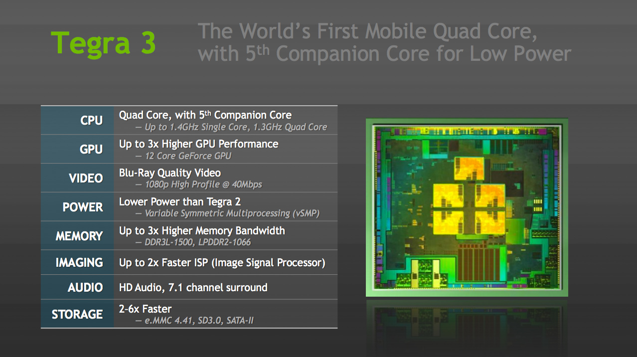
Tegra 3's GPU is very much an evolution of what we saw in Tegra 2. The GeForce in Tegra 2 featured four pixel shader units and four vertex shader units; in Tegra 3 the number of pixel shader units doubles while the vertex processors remain unchanged. This brings Tegra 3's GPU core count up to 12. NVIDIA still hasn't embraced a unified architecture, but given how closely it's mimicking the evolution of its PC GPUs I wouldn't expect such a move until the next-gen architecture - possibly in Wayne.
| Mobile SoC GPU Comparison | |||||||||||
| Adreno 225 | PowerVR SGX 540 | PowerVR SGX 543 | PowerVR SGX 543MP2 | Mali-400 MP4 | GeForce ULP | Kal-El GeForce | |||||
| SIMD Name | - | USSE | USSE2 | USSE2 | Core | Core | Core | ||||
| # of SIMDs | 8 | 4 | 4 | 8 | 4 + 1 | 8 | 12 | ||||
| MADs per SIMD | 4 | 2 | 4 | 4 | 4 / 2 | 1 | 1 | ||||
| Total MADs | 32 | 8 | 16 | 32 | 18 | 8 | 12 | ||||
| GFLOPS @ 200MHz | 12.8 GFLOPS | 3.2 GFLOPS | 6.4 GFLOPS | 12.8 GFLOPS | 7.2 GFLOPS | 3.2 GFLOPS | 4.8 GFLOPS | ||||
| GFLOPS @ 300MHz | 19.2 GFLOPS | 4.8 GFLOPS | 9.6 GFLOPS | 19.2 GFLOPS | 10.8 GFLOPS | 4.8 GFLOPS | 7.2 GFLOPS | ||||
Per core performance has improved a bit. NVIDIA worked on timing of critical paths through the GPU's execution units to help it run at higher clock speeds. NVIDIA wouldn't confirm the target clock for Tegra 3's GPU other than to say it was higher than Tegra 2's 300MHz. Peak floating point throughput per core is unchanged (one MAD per clock), but each core should be more efficient thanks to larger caches in the design.
A combination of these improvements as well as newer drivers are what give Tegra 3's GPU its 2x - 3x performance advantage over Tegra 2 despite only a 50% increase in overall execution resources. In pixel shader bound scenarios, there's an effective doubling of execution horsepower so the 2x gains are more believable there. I don't expect many games will be vertex processing bound so the lack of significant improvement there shouldn't be a big issue for Tegra 3.
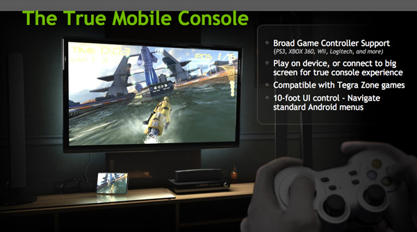
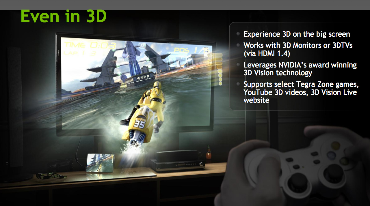
Ready for Gaming: Stereoscopic 3D and Expanded Controller Support
Tegra 3 now supports stereoscopic 3D for displaying content from YouTube, NVIDIA's own 3D Vision Live website and some Tegra Zone games. In its port of Android, NVIDIA has also added expanded controller support for PS3, Xbox 360 and Wii controllers among others.
Tegra 3 Video Encoding/Decoding and ISP
There's unfortunately not too much to go on here, especially not until we have some testable hardware in hand, but NVIDIA is claiming a much improved video decoder and more efficient video encoder in Tegra 3.
Tegra 3's video decoder can accelerate 1080p H.264 high profile content at up to 40Mbps, although device vendors can impose their own bitrate caps and file limitations on the silicon. NVIDIA wouldn't go into greater detail as to what's changed since Tegra 2, other than to say that the video decoder is more efficient. The video encoder is capable of 1080p H.264 base profile encode at 30 fps.
The Image Signal Processor (ISP) in Tegra 3 is twice as fast as what was in Tegra 2 and NVIDIA promised more details would be forthcoming (likely alongside the first Tegra 3 smartphone announcements).
Memory Interface: Still Single Channel, DDR3L-1500 Supported
Tegra 3 supports higher frequency memories than Tegra 2 did, but the memory controller itself is mostly unchanged from the previous design. While Tegra 2 supported LPDDR2 at data rates of up to 600MHz, Tegra 3 increases that to LPDDR2-1066 and DDR3-L is supported at data rates of up to 1500MHz. The memory interface is still only 32-bits wide, resulting in far less theoretical bandwidth than Apple's A5, Samsung's Exynos 4210, TI's OMAP 4, or Qualcomm's upcoming MSM8960. This is particularly concerning given the increase in core count as well as GPU execution resources. NVIDIA doesn't expect memory bandwidth to be a limitation, but I can't see how that wouldn't be the case in 3D games. Perhaps it's a good thing that Infinity Blade doesn't yet exist for Android.
SATA II Controller: On Die
Given Tegra 3 will find itself in convertible Windows 8 tablets, this next feature makes a lot of sense. NVIDIA's latest SoC includes an on-die SATA II controller, a feature that wasn't present on Tegra 2.


94 Comments
View All Comments
dagamer34 - Wednesday, November 9, 2011 - link
Using 40nm isn't an excuse when both Apple and Samsung use 45nm and have GPUs that trounce the Tegra 2 in real life and Tegra 3 on paper.eddman - Wednesday, November 9, 2011 - link
Yeah, and A5 is about 42%-43% bigger than tegra 3, an seems to be consuming more power and run hotter. I'd rather have less GPU power than that.Don't know anything about exynos' size and other characteristics.
Anand, do you have any such information on exynos?
MySchizoBuddy - Wednesday, November 9, 2011 - link
what's your source of A5 die size?eddman - Wednesday, November 9, 2011 - link
At first this: http://www.anandtech.com/show/4840/kalel-has-five-...Anand says tegra 3 is 30% smaller than A5, which means A5 is 42-43% bigger.
After your above comment, I searched a little bit, and noticed in the IT pro portal article linked in my other comment, it says 120 mm^2.
I also found these:
http://www.eetimes.com/electronics-news/4215094/A5...
http://www.notebookcheck.net/Analyst-explains-grap...
Here, it's 122 mm^2.
Now with the exact size known, it puts the A5 in an even worse situation, 50-52% bigger.
eddman - Wednesday, November 9, 2011 - link
Ok, it seems exynos' size is about 118 mm^2.http://www.itproportal.com/2011/06/07/exynos-soc-s...
http://www.businesswire.com/news/home/201107070061...
Considering that tegra 3 has 5 cores and yet is still much smaller, I might say nvidia has actually done some nice engineering here.
Wonder how much of that difference is because of 40 nm process vs. 45 nm. Probably not much, but what do I know. Can anyone do some calculations?
metafor - Wednesday, November 9, 2011 - link
It's really difficult to judge because they're from two different foundries. The minimum etch (e.g. 45nm, 40nm) isn't the only thing that affects die area. Some processes require stricter design rules that end up bloating the size of logic.Samsung uses Samsung semi's foundries while nVidia uses TSMC. It's difficult to say how they compare without two identical designs that have gone to fab on both.
Klinky1984 - Wednesday, November 9, 2011 - link
I think the 500Mhz companion core & proper power gating alleviates most of the concerns about power consumption.metafor - Wednesday, November 9, 2011 - link
Not really. It alleviates the concern of power consumption on light loads. While that is a big part of common usage and it's definitely a benefit to have great idle/light power, I still would like to have better battery life while I'm heavily using the device. For instance, while playing a resource-heavy game or going to pretty complex websites.One thing I do like is that they've improved the efficiency of the video decoder. This makes one of the most common use-cases (watching movies) less power-intensive.
SniperWulf - Wednesday, November 9, 2011 - link
I agree. I would rather they had made a strong dual-core and dedicate the rest of the die space to a second memory channel and a stronger GPUa5cent - Wednesday, November 9, 2011 - link
Qualcom is the only SoC manufacturer making the transition to 28nm anytime soon. Everyone else is shifting at the very end of 2012 (at the earliest).